
Boot Sequence of ESP32
When We start to learn a microcontroller or SoC, we want to write a lot of code quickly and make use of all the available features/peripherals. But I think acquiring proper knowledge of the boot sequence of an MCU is also very important.
I have seen embedded products getting stuck/hung in boot mode. Most of the time the reasons are developers not spending enough time on reading the datasheet & missing out on important hardware notes or fuse bit settings. Knowing the exact booting information will also help the programmer to plan or debug better. In this blog post, I would like to explain how ESP32 gets boot-ed. I hope the read will be an enjoyable one! :)
ESP32 Internal
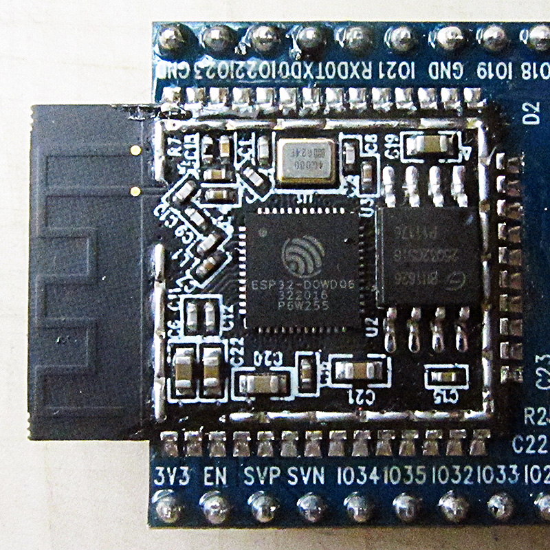
Here in the picture below you can see the internals of an ESP32 module . if you decap the metal plate of the module you will see inside It has mainly 2 silicon chips one is the esp32 mcu and other one is a SPI based flash chip.
Now let’s look into the following block diagram for better understanding what is inside.

Here you can see that the ESP32 module has one mcu and one flash chip, both being connected via SPI. The esp32 microcontroller itself has a small ROM . The First Stage bootloader resides in the ROM . It is pre-programmed by Espressif (the silicon vendor).
The important addresses are
| Type | Address Offset |
|---|---|
| Application | 0x10000 |
| Partition Table | 0x8000 |
| 2nd stage Bootloader | 0x1000 |
The microcontroller has 2 CPU , these are
- PRO CPU
- APP CPU
Partition Table & FLash
Now let’s understand the partition table . Just like we divide our laptop’s hard disks into different partitions for example Drive [ C: D: E:]. One can divide the SPI flash of the ESP32 module into multiple partitions. different partitions can hold different types of data (e.g. calibration data, filesystems, parameters storage, OTA backup etc).
Unlike other mcu manufacturers espressif gives us a lot of flexibility in flash space orientation provided the Flash is external to the mcu itself . Very clever and modular design! Obviously this type of SoC design has some drawbacks but we can talk about that later . Now back to partitioning . In order to implement the dividends A partition table needs to be flashed at memory address 0x8000. This table tells what kind of data gets into which partition. This can be configured using the menuconfig

Reset Sources
Before explaining the boot sequence we should know which are the reset sources of our mcu ESP32 microcontroller has the following reset sources
- Wake up from deep sleep
- Power on reset (POR)
- Watchdog (WDT)
- Software (SWT)
Flashing hardware tool Connection

The RTS & DTR lines of USB-UART chip CP2102 is connected to GPIO0 & EN pin of the mcu as shown in the above picture & below table
| ESP32 Pin | Serial Pin(CP2102) |
|---|---|
| EN | RTS |
| IO0 (GPIO0) | DTR |
Flashing command
When we build our project using idf.py of the esp-sdk, the built tool builds the bootloader binary file along with the application binary, for example during the build of the gpio example 2 bin files get generated named bootloader.bin & gpio.bin.
esptool.py -p /dev/ttyUSB0 -b 460800 --after hard_reset write_flash --flash_mode dio --flash_freq 40m --flash_size 4MB 0x8000 partition_table/partition-table.bin 0x1000 bootloader/bootloader.bin 0x10000 gpio.bin
Boot Sequence
Following the reset of any kinds listed above, ESP32 will go through the following bootup sequence.
-
MCU resets
-
PRO-CPU runs & does all the initialization while APP-CPU is held in reset
-
CPU jumps to Reset vector
-
Reset vector is located at address 0x40000400 in the ROM
-
Startup code(1st stage bootloader) is called from reset vector
-
1st stage bootloader checks Reset reason
-
1st stage bootloader checks if UART or SDIO (sd-card) download mode is requested or not , if so it waits for the incoming binary code to be downloaded (This event happens during flashing process)
-
Assuming flashing command is being executed and GPIO0 is held LOW on reset by the flashing hardware (CP2102) then The ESP32 will enter into the bootloader mode.
-
If the 1st stage bootloader finds that UART download should be performed then it does so and puts the received bootloader.bin at offset 0x1000 in flash. ( This bootloader is called the 2nd stage bootloader). then it writes the application binary at the pre-set offset Address (0x10000)
-
So once 1st stage bootloader finishes writing the binary data given by esptool.py, it jumps to 2nd stage bootloader.
-
Getting jumped from 1st stage bootloader, The 2nd stage bootloader takes in control and starts running, at start it prints some informations via UART0 , reads partition table from offset 0x8000 & prints the partition table
-
after 2nd stage bootloader gets done printing some useful information, PRO-CPU prints some other info and transfers the control over to the the APP-CPU
-
APP-CPU starts executing the Application binary machine instructions & Starts the FreeRtos Scheduler thus our application begins running
-
During operation / normal runtime If any of the reset sources triggers then all the sequence happens again.
-
If The First stage bootloader does not get any data over UART within a fixed time then timeout occurs and it jumps to the 2nd stage bootloader and all the subsequent steps occur as explained above.
I (74) boot: Chip Revision: 1
I (74) boot_comm: chip revision: 1, min. bootloader chip revision: 0
I (40) boot: ESP-IDF v4.1-dev-474-g2e6398aff 2nd stage bootloader
I (41) boot: compile time 18:30:23
I (41) boot: Enabling RNG early entropy source...
I (47) boot: SPI Speed      : 40MHz
I (51) boot: SPI Mode       : DIO
I (55) boot: SPI Flash Size : 4MB
I (59) boot: Partition Table:
I (62) boot: ## Label            Usage          Type ST Offset   Length
I (70) boot:  0 nvs              WiFi data        01 02 00009000 00006000
I (77) boot:  1 phy_init         RF data          01 01 0000f000 00001000
I (85) boot:  2 factory          factory app      00 00 00010000 00100000
I (92) boot: End of partition table
I (96) boot_comm: chip revision: 1, min. application chip revision: 0
I (191) boot: Loaded app from partition at offset 0x10000
I (191) boot: Disabling RNG early entropy source...
I (192) cpu_start: Pro cpu up.
I (196) cpu_start: Application information:
I (201) cpu_start: Project name:     gpio
I (205) cpu_start: App version:      v4.1-dev-474-g2e6398aff
I (212) cpu_start: Compile time:     Oct 28 2019 16:42:49
I (218) cpu_start: ELF file SHA256:  722f4baa50cdbbc9...
I (224) cpu_start: ESP-IDF:          v4.1-dev-474-g2e6398aff
I (230) cpu_start: Starting app cpu, entry point is 0x40080fec
0x40080fec: call_start_cpu1 at /home/hassin/esp/esp-idf/components/esp32/cpu_start.c:276

I (0) cpu_start: App cpu up.
I (240) heap_init: Initializing. RAM available for dynamic allocation:
I (298) cpu_start: Starting scheduler on PRO CPU.
I (0) cpu_start: Starting scheduler on APP CPU.
By embedding the 1st stage bootloader in the esp32 mcu, espressif has made programming of the module very easy. In addition, as the UART interface is chosen for the transfer, the whole process becomes much easier, not requiring complex tools like JTAG / ISP programmers. Still one can use the JTAG interface for programming / debugging but I will cover that in a later post.
References:
- https://docs.espressif.com/projects/esp-idf/en/latest/api-guides/general-notes.html
- https://github.com/espressif/esptool/wiki/ESP32-Boot-Mode-Selection
- https://docs.espressif.com/projects/esp-idf/en/latest/api-guides/partition-tables.html
- https://dl.espressif.com/dl/schematics/esp32_devkitc_v4-sch.pdf